 New Mould


 Plastic Products


 Feature Service
Mould Equipment
Feature Service
Mould Equipment

Anaheim Convention Center
Anaheim,CA,USA
Be Our Member to source precision machining parts!
TECHNICAL Resources DESIGN of Silicone Rubber Keypad
Design Silicone (DSW) is your trusted source for molded rubber parts, plastic injection molding, membrane switches, turn-key assemblies.
DSW work closely with the customer, the engineer and the production team to make design, rapid prototype, and produce your rubber parts completed to specifications and on-time.
If you need additional information please contact us directly at dsw@vip.163.com
SILICONE RUBBER BENEFITS
Silicone rubber is an excellent material for several reasons;
- ·Resistance to both high and low temperatures (-55° C to 250° C)
- ·Minimal noise generation due to soft and elastic contact structure
- ·Minimal abrasion and high resistance to SO2 and oxidation even in heavy humidity
In addition, silicone rubber offers several features that make its design and usage flexible;
- ·Design both tactile and linear feedback
- ·Translucent color is excellent for backlighting
- ·Cost effective
- ·Multi-color designs easily accommodated
- ·Water and contamination resistant
Dictionary of Terms Used
BASIC KEY CONSIDERATIONS
Key design will vary with the functional and aesthetic requirement of the application. It is possible to mold a key in almost any shape and to fit almost any configuration. It is important to remember that the key shape will affect the feel of the key. While a circular shaped standard key will have a consistent feel across the entire surface a half moon shaped key will respond different depending upon where the key is pressed.
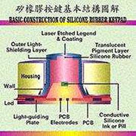
Once you have decided upon a key shape and layout. The next item to consider is the method for marking the rubber and creating legends. There are three common methods for marking keypads including printing, laser etching, and plastic key caps.
Printing
Printing is the most common method of marking rubber. The rubber is fixtured to flatten the key top then screen printed. There is no limit to the number of colors available. The arc of the key top determines how far printing must be set back from the edge of the key.
There are currently several options available for improving legend life with printed rubber.
- ·Plastic Key Caps – custom molded clear plastic is adhered over the legend or molded into the rubber
- ·Oil or Epoxy Coating – coating is deposited on the top surface of the key over printing, available in matte, semi-gloss, or gloss finish
- ·Drip Coating – drip coating can be hard or flexible. It adds a glossy layer over the key top. It can not be used on some keys with sharp angles. Hard coatings are subject to cracking if the key has large surface areas.
- ·Parylene Coating – offers the highest level of protection for a non-plastic coating. Parylene bonds to the rubber at the molecular level.
Laser Etching
Laser etching is especially well suited for applications where the keypad is backlit. Etching typically involves three production steps.
- ·Translucent rubber (any color) is sprayed with a translucent base coat ink which will be the legend color that is visible to the user.
- ·Rubber is sprayed with an opaque top coat ink which will be the overall color of the keypad.
Alternatively, you can decide to use a single translucent or opaque rubber ink and laser etch the legends revealing the color of the rubber that is used.
Plastic Key Caps
The longest lasting legend type is custom molded plastic. Plastic legends will not wear out. Many cell phone keypads are designed with plastic keys over rubber.
FUNCTIONAL DESIGN CONSIDERATIONS
Snap Ratio & Tactile Feel
The snap ratio of a keypad determines the tactile feel experienced by the user. The recommended snap ratio for designers to maintain is 40%-60%, if dropping below 40% the keys will lose tactile feel but have an increased life. Loss of tactile feel means the user will not receive a 'click' feedback during actuation.
Snap ratio is calculated by taking the [ACTUATION FORCE (F1) – CONTACT FORCE (F2)] / ACTUATION FORCE (F1).
The membrane shape and the size of any rubber key mat can be designed to achieve a variety of actuation forces and tactile responses. Most applications require a positive tactile feel and a long life. With these requirements, an actuation force of 125-150 grams and an accompanying snap ratio of 40%-60% is a good recommendation. Other combinations can be achieved by changing the contact stroke, actuation force, key shape and material hardness. RSPI works with customers to achieve the specifications required. Always remember to specify a higher actuation force for wider or taller keys.
Reducing Rocking Action
A common problem with rubber keypad design is the rocking action that can occur when a key is pushed. Rocking action can reduce the life of the keypad, make actuation difficult for the user, and cause other problems. The following suggestions will assist in reducing this problem.
- ·Add stabilizing posts on base of key
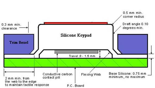
- ·Keep key stroke as near 0.8mm as possible
- ·Keep web length to a minimum
- ·Keep web angle close to 40
- ·Actuation force of 80-150 grams for keys 10-15 mm high and 150-175 grams for keys 15-25mm high
Return force should also be set at 30-35 grams to ensure that keys do not stick.
Switch Life
The web design and the durometer of the rubber are two factors that affect keypad longevity most. The design should reduce stress on the rubber if long life is desired. Using higher durometer silicone, increasing the actuation force, or increasing the stroke will all decrease the keypads life.
Rubber Hardness
Rubber hardness for a keypad can vary between 30 and 70 durometer (Shore A). Typically, most keypads are built between 40 and 60 durometer.
Minimum Key Height
For any design, calculate the minimum key height as follows; Keypad Base Thickness + Bezel Thickness + Stroke of Key + 0.5mm.
Contacts
The carbon pill is the most common contact because of its long life (>10 million actuations) and low resistance (<100W). The pills are usually circular with diameters ranging from 1.5-10mm and thickness from 0.4-0.6mm. Oval shaped pills are also available in a variety of sizes.
Printed carbon contacts are available in any shape however thickness is typically only 10-20 microns and resistance around 800W.
Dipped carbon contacts offer a compromise with any shape being available and contact resistance of <300W.
Printed Circuit Board Design
Rubber key mats themselves are very reliable in operation. However, when considering a PCB design, the environment that the keypads are used in must be considered to ensure the complete switching unit is reliable.
The choice of plating for the board is probably the most critical factor with the cheaper tin/lead solder boards not being recommended.
Gold plating over nickel plating is the preferred choice for board design with a recommended layer of 30-50 microns of gold and 100-200 microns of nickel giving a contact resistance of <100W.
Nickel plating is the next best option and the most commonly used; nickel offers good reliability and is more cost effective than gold over nickel. A plating level >200 microns is recommended for the best overall performance.
When designing shorting pads, always attempt to insert as many shorting paths as possible to increase switch reliability and ensure the pad size is never smaller than the carbon pill by a minimum of 1.25 times.
Flexible Printed Circuit Design
Rubber keypads are typically used with printed circuit boards. However, many rubber keypads are also used with flexible printed circuits.Flexible circuits can be made of polyester or copper.
MECHANICAL DRAWINGS
RSPI can estimate most rubber projects with a 2D drawing that shows the number of printed colors and the number of rubber colors that are used. When your design moves to production or if you need to receive more accurate pricing you should try to include the following information if applicable:
| Overall keypad dimensions | Base thickness |
| Key top outside dimensions | Overall key heights |
| Contact size | Mounting hole details |
| Mounting boss details | Dimensions (keypad and buttons) |
| Keypad/switch colors | Stroke/travel |
| Actuation force | Snap Ratio (optional) |
| Electrical specs | Material specs |
| Graphic color(s) | Printing artwork |
TYPICAL KEYBOARD SPECIFICATIONS
| Characteristics | Conductor | Insulator |
| Material | Carbon Pill | Silicone |
| Durometer (Shore A scale) | 65 +/-5 | 30-80 +/- |
| Tensile Strength (kg/cm2) | 60 | 65-85 |
| Tear Strength (kg/cm) | 15 | 10-15 |
| Compression set (%) | 20 | 11-22 |
| After 22 hrs at 175° C Specific gravity at 25° C |
1.18 | 1.11-1.18 |
| Contact Resistance | <200W at 12V dc 30mA |
| Insulations Resistance | >100W at 250V dc |
| Max contact loading | 21V dc 100mA |
| Strength | 20-25kv/mm |
| Constant | 26-35 MHz |
| Volume Resistance | >2 x 10¹² (W) |

